
 Electronic circuits are a key part of electronic devices, but they present unique challenges. They require precise integration of conducting, insulating, and semiconducting materials in two- and three-dimensional space to control the flow of electric current. The UES Biological & Nanoscale Technologies team worked with Government and Academia partners to approach this challenge in a new way in their latest work "Laser writing of electronic circuitry in thin film molybdenum disulfide: A transformative manufacturing approach."
Read also: A Novel Method for Characterization of Biotic-Abiotic Interactions
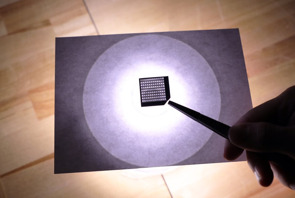
In this work, the team developed a new technique for rapidly producing functional patterns on an electronic chip. Instead of traditional methods, they applied a transformative manufacturing approach using laser processing to directly realize conducting, insulating and semiconducting phases within an amorphous molybdenum disulfide thin film precursor.
UES Scientist and lead author Drake Austin goes into further detail. "By focusing a relatively low power laser beam onto the a-MoS2 thin film in air, we are able to locally heat a small region of the sample to several hundred degrees Celsius. The time spent at this temperature could then be controlled by scanning the laser beam across the surface at varying speeds, causing the a-MoS2 to either crystallize into 2H-MoS2 or oxidize into MoO2 or MoO3. We then found that we could take advantage of the different electrical properties of these three chemical phases to 'laser-write' simple electronic devices."
This innovative approach shows promise in improving manufacturing speed and throughput. Beyond increasing efficiency, this transformative manufacturing approach also offers reconfigurability of the process. Without the need for expensive equipment and the many additive and subtractive steps tradition circuit design requires, this solution allows for more freedom of design.
This research was truly a team effort, with scientists from AFRL, Case Western Reserve University, University of Dayton, University of California Los Angeles, University of Cambridge, and UES, Inc.
Lucas Beagle, UES scientist, used his chemistry knowledge for species conversion in this study. He spoke to the value of this teamwork and collaboration in making this project successful. "The thing I enjoyed the most was how well we worked together as a team across the branch and directorate, as well as with our academic collaborators to bring this new technology to light. I enjoyed being able to lend my talents and share my experience in my discipline in order to contribute to the innovative research in a meaningful way."
Read more about this work on Materials Today.
Read also: Recent Biological & Nanoscale Technologies Research
Questions? Contact us here. Connect with us on Facebook, Twitter, LinkedIn, and Instagram.