
UES' Robo-Met team has completed work on a Phase I SBIR from the Defense Micro Electronics Activity (DMEA), to explore adaptation and use of the Robo-Met system in electronics delayering. Learn more about our strides in developing this new application below.
Read also: 2021 Research Using Robo-Met's Materials Analysis
Electronics Delayering
The miniaturization of portable electronic devices relies on complex integrated circuits (ICs) to accommodate a multitude of functions as devices shrink in size. Especially in a the context of the National Security Enterprise, the development, design, and failure analysis of chip-based components requires delayering with the goal of successfully removing layers of material to identify the areas of interest to image or analyze features in ICs. Reverse engineering and security analysis, which are other goals of such processes, are becoming increasingly challenging in terms of the resource burden on personnel and precision required. A system that can automate the routine metallographic aspects of delayering and enhance material removal precision and repeatability, as well as throughput - such as Robo-Met - is desirable.
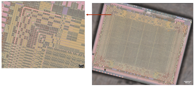 Fig. 1: Highly detailed Robo-Met image of a XILINX Spartan 3 series Field Programmable Gate Array (FPGA) IC 97 294912 8064 144-LQFP.
Technical Objectives
The Robo-Met.3D system, developed by UES, Inc. (UES) in conjunction with the Air Force Research Laboratory (AFRL) and the Naval Research Lab (NRL), offers several of the desired features outlined in the topic description as an accelerated development starting point. The system has many of the desired features requested by the Defense Microelectronics Activity (DMEA), leaving scope to develop to the remaining requirements. The technical objective of the Phase I program was to deploy the Robo-Met.3D serial sectioning system and the engineering expertise of the UES Team to execute a feasibility study of automatic serial sectioning an IC to an arbitrary metal layer in a planar manner that results in all vias being present, along with a relatively uniform interlayer dielectric material (ILD), and all metal lines beneath it.
Summary of Results
Starting from a system designed for bulk material delayering, the UES team achieved significant progress in the Phase I effort. UES demonstrated the feasibility of an automated robotic delayering system capable of:
- Handling IC chips and delayering them with submicron-level accuracy
- Adapting the system for submicron delayering, to show metallic layers, silicon/ILD materials, and leads/vias. The level of detail achievable with optical microscopy is remarkable (Fig. 1).
- Incorporating design improvements towards enhanced flatness and perpendicularity of polishing
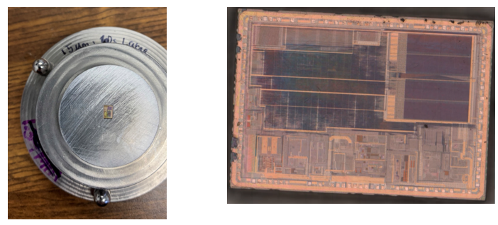
Fig. 2: Modified Sample Mounting and Metallic Cu Layer for a Texas Instruments CPUXV2 series Microcontroller IC
• Imaging using optical microscopy in the 50x–500x magnification range, including imaging with polarized and DIC modes (Fig. 3).
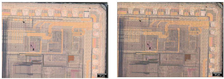
Fig. 3: Polarized Light (left) and DIC (right) images for Texas Instruments CPUXV2 series Microcontroller IC
• Evaluated feasibility and plans for both SEM integration and self-contained systems .
This Phase I outcome shows the viability of developing a system capable of validating the design of an entire IC by frontside serial sectioning, useful to DMEA and other stakeholders.
Video: Preview of Robo-Met.3D data on a XILINX Spartan 3 series Field Programmable Gate Array (FPGA) IC Copper Layers (~ 6 microns thick).
We gratefully acknowledge funding by DMEA SBIR Contract HQ072721P0034. We look forward to implementing these improvements in Phase II and beyond. Our customers love Robo-Met's low-touch and automated nature, which allows them to limit contact in their characterization labs. If you have expertise in microelectronics or in other applicable delayering areas, we would love to initiate a conversation and partner with you. Contact us to get started!
You can learn more about Robo-Met and how it can help you solve your materials challenges here. Have particular material challenges you’d like to discuss with our experts? Contact us here.
Questions? Contact us here. Connect with us on Facebook, Twitter, LinkedIn, and Instagram.