
UES' Robo-Met team has made won a Phase I SBIR from the Defense Micro Electronics Activity (DMEA), to explore adaptation and use of the Robo-Met system in electronics delayering. Learn more about our strides in developing this new application below.
Read also: 2021 Research Using Robo-Met's Materials Analysis
 Electronics Delayering
The miniaturization of portable electronic devices relies on complex integrated circuits (ICs) to accommodate a multitude of functions as devices shrink in size. Especially in a the context of the National Security Enterprise, the development, design, and failure analysis of chip-based components requires delayering with the goal of successfully removing layers of material to identify the areas of interest to image or analyze features in ICs. Reverse engineering and security analysis, which are other goals of such processes, are becoming increasingly challenging in terms of the resource burden on personnel and precision required. A system that can automate the routine metallographic aspects of delayering and enhance material removal precision and repeatability, as well as throughput - such as Robo-Met - is desirable.
DMEA SBIR Phase I Award
In early exploratory work with an ST Microelectronics MEMS Accelerator 2-16G 12C SP I 16LGA off the shelf device, we had been able to demonstrate the ability to fine-tune Robo-Met workflows to achieve micron-order removal rates consistently in heterogeneous structures. In addition, the metallic lead structures etc. were clearly discernible and segmentable (Fig. 1).
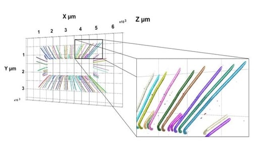 Fig. 1: Delayering detail and metallic leads in MEMS Accelerator
On the basis of this early success, we proposed to DMEA's SBIR topic on to develop a Microelectronic Automated Serial Sectioning System (MASS). Key objectives would be to deploy the Robo-Met.3D serial sectioning system and the engineering expertise of the UES Team to execute a feasibility study of automatic serial sectioning an IC to an arbitrary metal layer in a planar manner that results in all vias being present, along with a relatively uniform interlayer dielectric material (ILD), and all metal lines beneath it. We were thrilled to be awarded DMEA Contract HQ072721P0034 to undertake this work. Even under routine optical microscopy, the level of detail resolvable in a chip is impressive (Fig. 2).
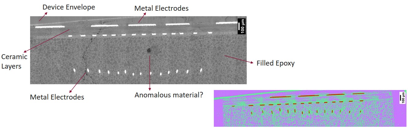
Fig. 2: MEMS Accelerator interior features
Robo-Met Modifications for Electronics
While we think we have a strong contender in the Robo-Met system, many modifications could be needed to accommodate the needs of the microelectronics community. For example, the requirement for precision planarity exceeds the requirements commonly encountered by the materials development community. The need to resolve features on the order of nanometers will also necessitate the integration of a scanning electron microscope - which is feasible and has been implemented at the AFRL and the NRL (Fig. 3).
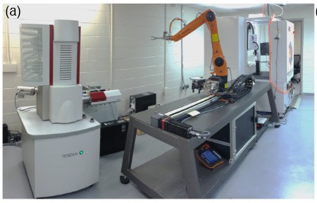 Fig. 3: Robo-Met integrated with Automatic Sample Transfer to an SEM, NRL
Given UES' research orientation, we're looking forward to tackling the challenges we will encounter. Our customers love Robo-Met's low-touch and automated nature, which allows them to limit contact in their characterization labs. If you have expertise in microelectronics or in other applicable delayering areas, we would love to initiate a conversation and partner with you. Contact us to get started!
You can learn more about Robo-Met and how it can help you solve your materials challenges here. Have particular material challenges you’d like to discuss with our experts? Contact us here.
Questions? Contact us here. Connect with us on Facebook, Twitter, LinkedIn, and Instagram.